
 Orders@pcbamake.com


High Density Interconnect (HDI) PCBs are becoming a growing part of the printed circuit board
industry. Request an HDI PCB quote today!
GET PRICING AND LEAD TIME

 PCB")
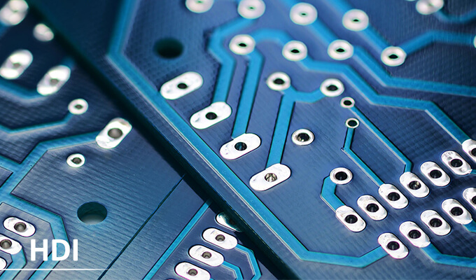
HDI PCB represents High Density Interconnect Printed Circuit Board. It is an advanced technology in multilayer circuit boards and are among the fastest-growing solutions in the industry. These boards sit on a high-density substrate with routing and pad connections compared to standard PCBs.
Designed for compact and high-performance applications, HDI PCBs feature significantly higher wiring density than conventional boards. They are typically based on a laminated structure with double-sided or multilayer cores, making them lighter, thinner, shorter, and smaller.
HDI technology enables greater miniaturization of electronic products while delivering enhanced performance and efficiency, meeting the demands of modern, high-tech designs.
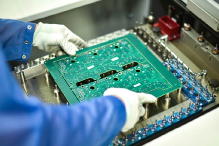
If you are developing complex electronic products, you need durable, reliable, and high-performance HDI PCBs. With PCBAMake’s advanced HDI manufacturing capabilities, we deliver customized solutions tailored to your specific needs.
Since 1996, PCBAMake has been committed to supporting innovation and meeting the challenges of increasingly sophisticated technologies. One of our core values is uncompromising quality in every circuit board we produce. To ensure this, we apply rigorous quality control measures at every stage of the manufacturing process, including:
We're capable of manufacturing HDI PCB up to 40 layers in various structures, check the following table for our available HDI PCB structures:
| HDI Structures | Type of Microvias | Mass Production | Small /Middle Batch | Prototype | Layers Availible |
|---|---|---|---|---|---|
| 1+N+1 | Blind vias | Yes | Yes | Yes | 4 layers+ |
| 2+N+2 | Blind/Buried staggered vias | Yes | Yes | Yes | 4 layers+ |
| 2+N+2 | Blind/Buried stacked vias | Yes | Yes | Yes | 6 layers+ |
| 3+N+3 | Blind/Buried staggered vias | / | Yes | Yes | 8 layers+ |
| 3+N+3 | Blind/Buried Stacked Vias | / | / | Yes | 8 layers+ |
| ITEM | Capability |
| Layers | 1-28 |
| Thicker Copper | 1-6OZ |
| Products Type | HF(High-Frequency)&(Radio Frequency) board, Impedance controlled board , HDI board ,BGA& Fine Pitch board |
| Solder Mask | Nanya&Taiyo ;LPI & Matt Red, green, yellow,white, blue,black. |
| Base material | FR4(Shengyi China、ITEQ, KB A+,HZ), HI-TG, FR06, Rogers,Taconic、Argon、Nalco、Isola and so on |
| Finished Surface | Conventional HASL,Lead-free HASL,Falsh Gold, ENIG (Immersion Gold)OSP(Entek), Immersion Tin,ImmersionSilver,Hard Gold |
| Selective Surface Treatment |
ENIG(immersion Gold)+OSP, ENIG(immersion Gold)+Gold Finger,Flash Gold +Gold Finger, immersion Silver+ Gold Finger, Immersion Tin+Gold Finger |
| Technical Specification | Minimum line width/gap:3.5/4mil(laser drill) Minimum hole size:0.15mm(mechanical drill)/4mil(laser drill) Minimum Annular Ring: 4mil Max Copper thickness: 6OZ Max Production size:900×1200mm Board Thickness:D/S: 0.2-7.0mm, Multilayers:0.40-7.0mm, Min Solder Mask Bridge:0.08mm Aspect ratio: 15:1 Plugging Visa capability: 0.2-0.8mm |
| Tolerance | Plated holes Tolerance:0.08mm(min±0.05) Non-plated hole tolerance:0.05min(min+0/-0.05mm or +0.05/-0mm) Outline Tolerance:0.15min(min±0.10mm) Functional test : Insulating resistance : 50 ohms (mormality) Peel off strength: 1.4N/mm Thermal Stress test :2650c,20 seconds Solder mask hardness:6H E-Test voltage :500V+15/-0V 30S Warp and Twist: 0.7% (semiconductor test board≤0.3% ) |


Over 20 years of PCB experience
PCBAMake has been delivering high-density interconnect printed circuit boards for more than 20 years, and we believe no order is too small, and no tolerance is too tight.Pair that with competitive pricing, quick quotes and response times, domestic and offshore manufacturing and an unprecedented level of flexibility, and you have a winning combination for all your HDI PCB needs.
Benefits
Shorter PCB manufacturing time-to-market and enhanced machine performance for Flip Chip, BGA, MCM, SIP technologies.
Advanced technology
Ultra thin cores, fine line geometries and alternative via methods for improved thermal transfer for thermal PCBs.In compliance with 20um circuit geometries, 30um dielectric layers, 50um laser vias and 125um bump pitch processing.
Short delivery time
Allows reducing the lead times by combining the manufacturing capabilities with a profound understanding of high speed digital and high frequency RF package requirements.
Better design
Increases the area for PCB designer to place electronical components and also enhances faster signal transmission and reduced signal loss.Our high HDI PCB boards have the technology-driving capabilities to bring applications in a large number of industries including but not limited to semiconductor test equipment, military weapons, medical, and aerospace.
HDI any-layer connect printed circuit boards are the next technological enhancement of HDI microvia PCBs: all the electrical connections between the individual layers consist of laser-drilled microvias. The main advantage of this technology is that all the layers can be freely interconnected.
HDI board is the most sophisticated circuit board in the PCB board, and its board making process is also the most complicated. Its core steps mainly include the formation of high-precision printed circuits, the processing of micro-via holes, and the electroplating of surfaces and holes.
Ultra-fine circuit processing
With the development of science and technology, some high-tech equipment is becoming more and more miniaturized and sophisticated, which requires higher and higher requirements for the HDI boards used. The line width/line spacing of HDI circuit boards of some devices has developed from the early 0.13 mm (5 mil) to 0.075 mm (3 mil), and has become the mainstream standard. The higher and higher line width/line spacing requirements bring the most direct challenge to the graphic imaging in the PCB manufacturing process.
The current formation process of fine lines includes laser imaging (pattern transfer) and pattern etching. Laser direct imaging (LDI) technology is to directly scan the surface of the copper clad laminate with photoresist to obtain the refined circuit pattern. The laser imaging technology greatly simplifies the process and has become the mainstream in HDI PCB plate making. process technology.
Micropore processing
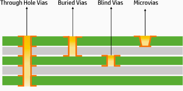
An important feature of HDI circuit boards is that they have micro vias (diameter ≤0.10 mm), which are all buried blind via structures.
Buried blind vias on HDI boards are currently mainly processed by laser.
Compared with laser drilling, mechanical drilling also has its own advantages. When laser processing through holes in epoxy glass cloth dielectric layer, due to the difference in ablation rate between the glass fiber and the surrounding resin, the quality of the hole will be slightly poor, and the residual glass fiber filaments on the hole wall will affect the reliability of the through hole. . Therefore, the advantages of mechanical drilling at this time are reflected. In order to improve the reliability and drilling efficiency of PCB boards, laser drilling and mechanical drilling technologies are steadily improving.
Through metallization
The biggest challenge of through-hole metallization is that it is difficult to achieve uniform plating. For the deep-hole electroplating technology of microvias, in addition to the use of an electroplating solution with high dispersibility, the plating solution on the electroplating device should be upgraded in time. This can be done through strong mechanical stirring or vibration, ultrasonic stirring, and horizontal spraying. In addition, the humidity of the through-hole wall must be increased before plating.
In addition to process improvements, HDIs’ through-hole metallization method has also seen major technological improvements: these include chemical plating additive technology, direct electroplating technology, etc.
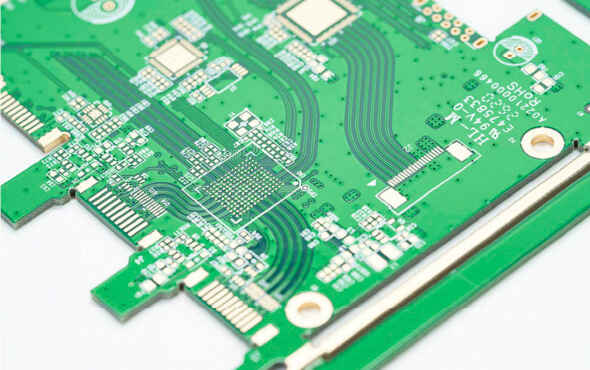
HDI PCB is a compact circuit board designed for small volume users. Compared with ordinary PCBs, the most notable feature of HDI PCB is the high wiring density. The HDI PCB board is based on the traditional double-sided board as the core board, which is continuously laminated. Compared with the traditional circuit board, the HDI PCB circuit board has the advantages of "light, thin, short and small".
The electrical interconnection between the board layers of HDI PCB is realized through conductive through holes, buried holes and blind holes. Its structure is different from ordinary multilayer PCB circuit boards. A large number of micro-buried blind holes are used in HDI PCB boards.
HDI PCB can not only enable more miniaturization of end product designs, but also meet higher standards of electronic performance and efficiency at the same time. The increased interconnect density of HDI PCB allows for enhanced signal strength and improved reliability.
These features give the HDI PCBs a higher circuitry density as compared to regular PCBs.
* Only zip or rar files accepted. Max 18MB.
Delivery Services

Verified by

Link Us on


