
 poe@pcbamake.com


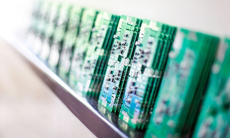
The OSP board surface treatment process is a PCB board surface treatment technology that forms an organic protective film on the PCB surface to protect the PCB surface metal and prevent oxidation and corrosion. The protective film is composed of an organic substance that can form a thin protective layer on the PCB surface. This is a common surface treatment process during PCB processing.
The role of OSP
The function of OSP PCB is to protect the metal on the PCB surface by forming an organic protective film on the PCB surface, preventing oxidation and corrosion, while ensuring good welding performance on the PCB surface. This organic film can prevent the inner copper foil from being oxidized before welding the circuit board. During welding, this film will evaporate once heated, and the solder can weld the copper wires and components together.
OSP panel surface treatment has the following advantages:
1. Cheaper because organic matter is used instead of metal.
2. Able to provide good welding performance and reliability.
3. Environmentally friendly because traditional surface treatment methods such as hot tin protective layer (HASL) or electroplating gold (ENIG) are not used.
However, OSP board surface treatment also has some disadvantages:
1. Transparent and colorless, it is difficult to inspect and it is difficult to tell whether it has been processed by OSP.
2. OSP itself is insulated and non-conductive, which will affect electrical testing. In this way, the test points must open a stencil and print solder paste to remove the original OSP layer before contacting the pin points for electrical testing.
3. Not resistant to corrosion and easily affected by acid and temperature. When used for secondary reflow soldering, it needs to be completed within a certain period of time. Usually the effect of the second reflow soldering will be relatively poor. If the storage time exceeds three months, it must be resurfaced and must be used within 24 hours after opening the package.
If an OSP circuit board is exposed to the air for more than ten days, components cannot be soldered.
The above is an introduction to OSP surface treatment. If you want to know more, you can follow PCBAMake. If you need to know more technical knowledge about PCB proofing, SMT patching, and PCBA processing, please leave a message to get it!If you have PCB/PCBA/OEM/ODM needs, please contact us, We will reply within 2 hours, and complete the quotation within 4 hours or less upon request.
Delivery Services

Verified by

Link Us on


