- Home
- About us
- Products
- PCB Fabrication
- PCB Assembly&OEM
- Quality
- Blogs
- Contact
One-Stop Turnkey PCB Assembly Manufacturer
PCB Assembly&OEM
When many people are initially understood by the PCB circuit board, they will be scared by the various layers of the circuit board. Each layer has its own names and functions. The division of labor is strict and the content is complicated. Today, let Pcbamake introduce it to you!

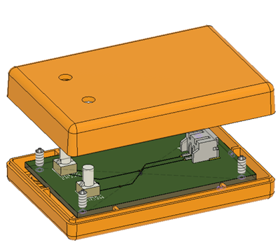
1. MeChanical, as the names of the names, are used for mechanical molding, that is, the appearance of the entire PCB. In fact, when we talk about the mechanical layer, we refer to the appearance structure of the entire PCB. It can also be used to set up the shape size, data mark, alignment mark, assembly description and other mechanical information of the circuit board. The information changes according to the requirements of the design company or PCB manufacturer. In addition, the Mechanical layer can be connected to other layers to output together.
2. Keep Out Layer, which is used to define components and wiring areas that can be effectively placed on the circuit board. Draw a closed area as an effective area for wiring. It cannot be automatically deployed and wiring outside this area. When we lay a copper with electrical characteristics, the wiring layer is prohibited from defining the boundary, that is, after we first define the prohibited wiring layer, in the future laying process, we cannot lay the electrical lines on the prohibition to prohibit. Outside the boundary of the wiring layer. The prohibited layer is usually used as a mechanical layer, which is actually wrong. Therefore, it is recommended that you distinguish it, otherwise the board factory will change the attribute for you every time it is produced.

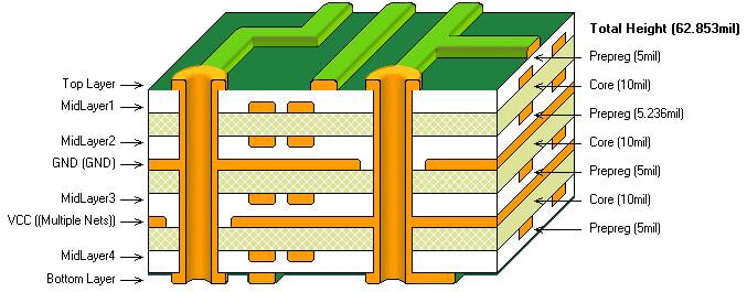
3. Signal layer: The signal layer is mainly used to arrange the wires on the circuit board. Including Top Layer (top layer), Bottom Layer (bottom layer) and 30 MidLayer (middle layer). The top layer and the Bottom layer placed device, the inner layer is carried out.
4. Top Paste and Bottom Paste are top layers, bottom pads steel mesh, and the size of the pads is as large as the size of the pads. This is mainly because we can use these two layers to make the steel mesh when we do SMT. It just digs a pad-sized hole on the Internet. We put this steel mesh on the PCB board and brush the tin paste with a brush with a tin paste, as shown in Figure 2-1.
5. Top Solder and Bottom Solder ,This is a welder -resistant layer to prevent green oil coverage. We often say "open windows", conventional copper or wiring are covered with green oil by default. If you deal with it, you will prevent the green oil from covering it, and the copper will be exposed.

6. InternaL Plane Layer (internal power/ground floor): This type of layer is only used for multi -layer boards, mainly used to arrange power cords and ground wires. We call it a double -layer board, four -layer board and six -layer board, usually referring to the number of signal layers and the number of internal power/ground layers.
7. Silkscreen layer: Silk printing layer is mainly used to place printing information, such as the contour and labeling of the component, various annotated characters, etc. Altium provides TOP Overlay and Bottom Overlay, two wire printing layers, and placed the top wire printed files and underlying wire printing files respectively.
 8. Multi Layer: The pads and penetrating pores on the circuit board should penetrate the entire circuit board, and establish an electrical connection relationship with different electrical shift layers. Therefore, the system specifically sets up an abstract layer -multi -layer. Generally, the pads and holes are set on the multi -layer. If this layer is turned off, the pads and perforated cannot be displayed.
9. DRILL DRAWING: Drilling information in the process of circuit board manufacturing (such as a pad, a hole is required). Altium provides two drilling layers: Drill Gride (drilling indicator diagram) and Drill Drawing (drilling diagram).
If you have PCB/PCBA/OEM/ODM needs, please contact us, We will reply within 2 hours, and complete the quotation within 4 hours or less upon request.