
 poe@pcbamake.com


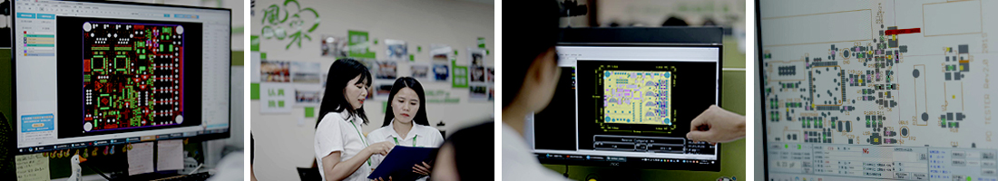
PCBA is the abbreviation of Printed Circuit Board Assembly in English. It is the entire process of PCB blank board through SMT loading, or PCB bare board through DIP plug-in, referred to as PCBA.
Key processes of PCBA manufacturing
1. Design and engineering preparation
Schematic design: Use EDA tools such as Altium Designer, KiCad or Cadence to create circuit schematics.
📌 Expert advice: Before submitting design files, you can conduct a DFM review with your PCBA supplier to reduce the cost of later modifications.
Substrate selection: FR-4 (standard), high-frequency materials (such as Rogers) or flexible PCB.
Lamination and etching: Circuit traces are formed through photolithography.
Drilling and copper plating: Create through holes and vias to achieve inter-layer connections.
Solder mask and silk screen: add protective layer and component identification.

3. Component procurement and verification
Component procurement: purchase high-quality components from reliable suppliers to avoid delays and defects.
BOM (Bill of Materials) management: ensure all components meet specifications to avoid supply chain delays.
Component verification: check authenticity (especially key IC chips) to avoid counterfeit components.
🌍 For areas with high environmental protection requirements, it is recommended to choose environmentally friendly components that comply with RoHS and REACH standards.

4. SMT patch and through-hole assembly
Solder paste printing: apply solder paste to specific areas of the PCB to prepare for component placement. The solder paste is accurately applied to the pad through the steel mesh.
Pick-and-Place: Place surface mount components (SMD) at high speed and accurately and quickly place components on the circuit board. .
Reflow soldering: melt the solder paste at high temperature to form reliable solder joints, thereby fixing the components in place.
Through-hole component (THT) assembly: wave soldering or manual soldering (for large-size components).

5. Testing and Quality Control
AOI (Automated Optical Inspection): Check for soldering defects (such as cold solder joints, short circuits).
Functional Test (FCT): Simulate the actual working environment to ensure product performance and ensure complete functionality before shipment.

6. Packaging and Delivery
Anti-static Packaging: Clean, label, and use anti-static (ESD) protection measures to package finished circuit boards to ensure safe delivery. Avoid static damage during transportation.
Compliance Labels: CE, FCC and other certification marks (according to target market requirements).
How to Choose a PCBA Manufacturer
Choosing the right PCBA manufacturer ensures quality, reliability, and scalability. You need to pay attention to the following points:
Experience and expertise: Check the manufacturer's experience cases in your industry (such as medical, automotive electronics).
Certification standards: ISO 9001 or IPC and other certifications.
Supply Chain Stability: Ensure reliable component procurement channels to avoid delivery delays.
Design Issues: Conduct a comprehensive DFM review to identify problems early.
Quality Control: Ensure rigorous testing to prevent product failures.

Why PCBAMake?
At PCBAMake, we provide high-quality PCBA services customized to your needs:
Global support for customers.
PCBA is the backbone of modern electronics. Choosing the right partner, you can bring your products to market faster and with more confidence.
📞 Contact us now for a free DFM analysis and quote!
If you have PCB/PCBA/OEM/ODM needs, please contact us, We will reply within 2 hours, and complete the quotation within 4 hours or less upon request.
Delivery Services

Verified by

Link Us on


