
 Orders@pcbamake.com

Learn about HDI PCB details and applications
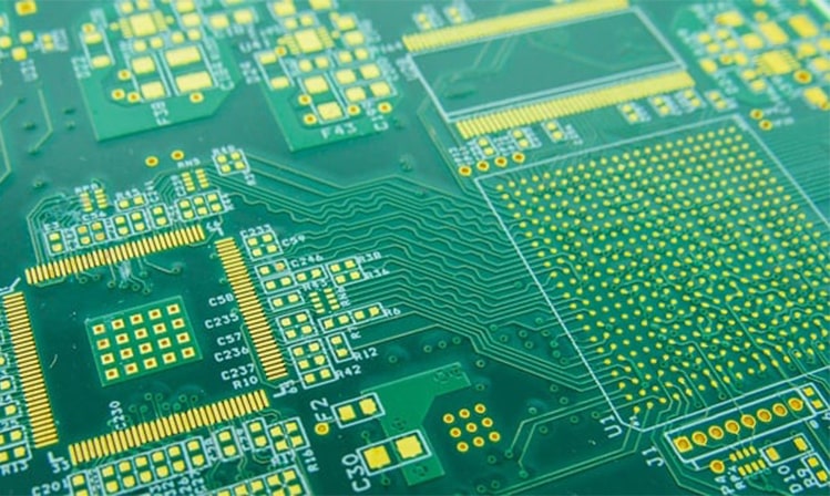
HDI PCB is a high -density interconnection board. It is a circuit board with a relatively high circuit distribution density using micro -blind holes and buried holes. HDI PCB can save PCB wiring area, greatly improve the density of components, and improve the performance of radio frequency interference/electromagnetic wave interference/static release.
The advantage of HDI PCB
Compared with traditional PCB, HDI PCB has many advantages, which has favored them in many applications. The main benefits are: high reliability, high density interconnection, smaller size, reducing weight, lower capacitance and inductance, higher performance, height customization.
HDI PCB application field:
There are mainly the following categories in the application field of HDI PCB:
Digital products such as smartphones, tablets, wearable devices, etc. These products require high -density circuit boards to achieve more functions and smaller size.
Motor electrons, such as instrument panels, navigation systems, security control systems, etc. These systems require high -speed, high reliability and high temperature tolerance circuit boards.
Medical equipment, such as implants, monitors, CT scans, etc. These equipment requires high transmission rates and small -sized circuit boards.
Chip packaging, such as BGA, CSP, MCM, etc. These packaging needs to be used directly for the circuit board with chips, which can provide functions such as packaging, electrical connection, protection, heat dissipation.
Other high -end electronic devices, such as laptops, digital cameras, 4G network communication, aircraft parts, etc. These devices require high -density circuit boards to improve signal integrity, reduce power consumption and reliability.
The advantages and challenges of HDI PCB are mainly the following points:
Advantage:
HDI PCB can improve line density, achieve more functions and smaller size.
HDI PCB can reduce the cost of PCB, especially when the density of PCB increases more than eight layers.
HDI PCB can improve electrical performance and signal correctness, reduce signal flight time and power consumption, and improve problems such as radio frequency interference, electromagnetic wave interference, and electrostatic release.
challenge:
The design and manufacturing process of HDI PCB is more complicated than ordinary PCB, and requires higher technical levels and stricter quality control.
The design and manufacturing process of HDI PCB needs to consider multiple factors, such as layers, materials, pore types, width and spacing, reliability assessment, DFM requirements, etc.
HDI PCB's testing and maintenance is also more difficult than ordinary PCB, and it requires more advanced equipment and tools.
How HDI PCB meets the manufacturer's DFM requirements, mainly in the following aspects:
1. Understand the capabilities and restrictions of the manufacturer, including material selection, pore type, width and spacing and spacing, impedance control, ring holes and vertical ratio.
2. Use design rules and online DRC engines to set up and check DFM requirements in the design software to avoid design characteristics that are not compliant.
3. Keep communication with the manufacturer, and timely obtain information such as electrical medium data, impedance curves, and reliability evaluation to create a suitable PCB stack layer.
4. Optimize layout and wiring, consider factors such as stacking layers, over -hole architecture, parts placement, and BGA fan, and improve line density and signal integrity.
For more questions about HDI PCB, you can access www to learn more. You can also communicate with our online customer service. We will immediately reply to you when we see that the information will be responded.
If you have PCB/PCBA/OEM/ODM needs, please contact us, We will reply within 2 hours, and complete the quotation within 4 hours or less upon request.
Delivery Services

Verified by

Link Us on


