What is Impedance Controlled PCBs
What is characteristic impedance? What should I do if the PCB design impedance is discontinuous?
One-stop PCBA intelligent manufacturing manufacturer will tell you today what to do if the PCB design impedance is discontinuous? How to solve the problem of PCB design impedance discontinuity. Everyone knows that PCB design impedance must be continuous. But there are always times when the impedance cannot be continuous in PCB design.
What is Controlled Impedance PCB?
Characteristic impedance: Also known as "characteristic impedance", it is not a DC resistance and is a concept in long-term transmission. In the high-frequency range, during signal transmission, where the signal edge arrives, an instantaneous current will be generated due to the establishment of an electric field between the signal line and the reference plane (power supply or ground plane).
If the transmission line is isotropic, then as long as the signal is transmitting, there will always be a current I, and if the output voltage of the signal is V, during the signal transmission process, the transmission line will be equivalent to a resistance with a size of V/I , call this equivalent resistance the characteristic impedance Z of the transmission line.
During signal transmission, if the characteristic impedance on the transmission path changes, the signal will be reflected at nodes with discontinuous impedance.
What factors affect characteristic impedance?
Factors that affect characteristic impedance include: dielectric constant, dielectric thickness, line width, and copper foil thickness.
Solutions to the problem of impedance discontinuity in PCB design
1. Gradient line
Some RF devices have small packages, and the SMD pad width may be as small as 12mils, while the RF signal line width may be more than 50mils. Gradient lines must be used to prohibit sudden changes in line width.
2. corner
If the RF signal lines are run at right angles, the effective line width at the corners will increase and the impedance will be discontinuous, causing signal reflection. In order to reduce discontinuity, there are two methods to process corners: chamfering and rounding. The radius of the arc angle should be large enough. Generally speaking, it should be ensured: R>3W.
3. Large pad
When there is a large pad on a 50 ohm fine microstrip line, the large pad acts as a distributed capacitance, destroying the characteristic impedance continuity of the microstrip line. Two methods can be used to improve it at the same time: first, thickening the microstrip line dielectric, and secondly hollowing out the ground plane under the pad, both of which can reduce the distributed capacitance of the pad.
4. Vias
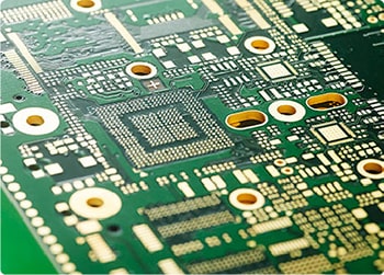
Vias are metal cylinders plated outside the holes between the top and bottom layers of a circuit board. Signal vias connect transmission lines on different layers. Via stub is the unused portion of a via. Via pads are donut-shaped pads that connect vias to top or internal transmission lines. Isolation pads are annular voids within each power or ground plane to prevent shorts to the power and ground planes.
5. Through-hole coaxial connector
Similar to via-hole structures, through-hole coaxial connectors also have impedance discontinuities, so the solution is the same as with via-holes. The common methods to reduce the impedance discontinuity of through-hole coaxial connectors are also: using diskless technology, appropriate outlet methods, and optimizing the anti-pad diameter.
Regarding what is characteristic impedance? What to do if PCB design impedance is discontinuous? If you want to know more, you can follow PCBAMake. If you need to know more technical knowledge about PCB manufacturing proofing, SMT patching, and PCBA processing, welcome Leave a message to get it!


