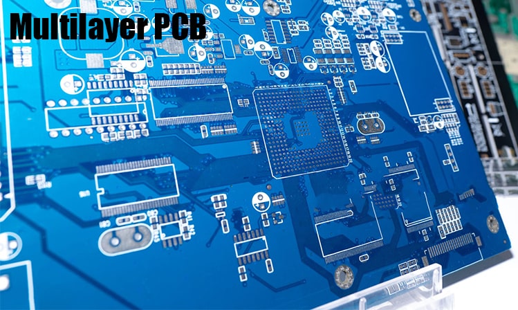
Why Multilayer PCBs Matter: Manufacturing Insights and Key Applications
As electronic products become smaller, faster, and more integrated, traditional single-layer and double-layer PCBs are no longer enough. Multilayer PCBs were developed to solve space, performance, and signal challenges that modern devices demand. This article explains why multilayer PCBs are needed, the problems they solve, how they are manufactured, and where they are commonly used.
Why Do We Need Multilayer PCBs?Space LimitationsWith compact device designs, board real estate is limited. Multilayer PCBs allow more routing channels without expanding surface area. Vertical stacking replaces horizontal expansion.
Complex CircuitsHigh-density components such as processors, FPGAs, memory chips, and RF modules require more signal layers and better power distribution. Multilayer boards make these layouts possible.
Signal IntegrityHigh-speed signals need controlled impedance, shorter routing paths, and solid reference planes. Extra layers help maintain signal quality and reduce crosstalk.
EMI/EMC ControlDedicated ground and power planes reduce electromagnetic interference and improve shielding performance.
Thermal & Power ManagementComplex circuits generate more heat and draw higher currents. Multilayer boards provide better copper distribution and heat dissipation paths.

What Problems Do Multilayer PCBs Solve?Limited routing space → Adds more layers without increasing size
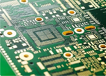
High component density → Supports BGA, fine-pitch ICs, and HDI layouts
Poor signal performance → Enhances impedance control and signal return paths
EMI issues → Improves layer isolation and grounding
Unstable power delivery → Enables solid power planes and shorter connections
Thermal buildup → Provides better copper balance and heat spreading
How Multilayer PCBs Are Manufactureda. Inner Layer Imaging & EtchingCopper is patterned to form inner circuits.
b. Layer Alignment & LaminationCore layers are stacked with prepregs and bonded under heat and pressure.
c. Drilling & Via PlatingThrough-holes or laser vias connect the layers electrically.
d. Outer Layer Imaging & EtchingTop and bottom layers are formed with the same precision.
e. Surface FinishingCommon finishes: ENIG, HASL, OSP, immersion silver.
f. Solder Mask & PrintingMask protects copper traces, silkscreen marks components.
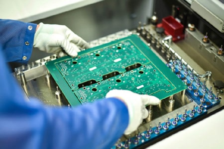
g. Testing & Final InspectionElectrical test ensures continuity and no shorts before packing.
Common ApplicationsTelecom & Networking5G modules, routers, communication base stations.
Industrial ElectronicsAutomation controllers, power systems, measurement devices.
AutomotiveADAS, in-vehicle displays, EV control units.
Medical EquipmentPortable monitors, diagnostic systems, imaging hardware.
Consumer ElectronicsLaptops, tablets, wearables, smart home devices.
Design Tips for Better PerformanceDefine the stack-up early for impedance and routing balance
Separate power, ground, and high-speed signal layers
Use blind, buried, or microvias when needed
Verify manufacturability with your PCB supplier
Work with the Right ManufacturerMultilayer PCBs involve tight tolerances, accurate lamination, and precision drilling. An experienced manufacturer can help reduce defects, improve yield, and shorten lead time—from prototypes to mass production.

