- Home
- About us
- Products
- PCB Fabrication
- PCB Assembly&OEM
- Quality
- Blogs
- Contact
One-Stop Turnkey PCB Assembly Manufacturer
PCB Assembly&OEM
A Detailed Explanation of Ultra-Small Surface Mount Components in PCB Manufacturing
In the PCB manufacturing industry, with the miniaturization and high integration of electronic products, the use of 0201 SMD packaging is becoming increasingly common, especially in high-density PCBA and precision SMT assembly projects.
What is 0201 SMD Packaging?
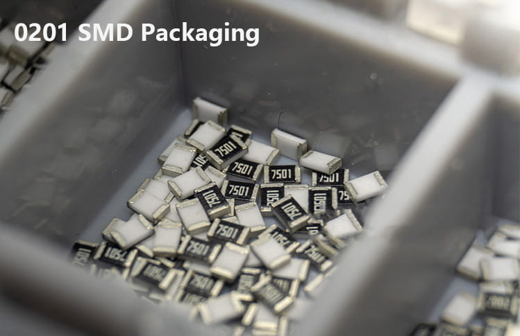
0201 SMD packaging is an ultra-small surface mount component packaging size standard, mainly used for passive components such as surface mount resistors and capacitors.
Package size: approximately 0.6 mm × 0.3 mm
One of the smallest commonly used SMD packages currently in mass production
Widely used in high-density PCB and precision PCBA projects
In actual PCB manufacturing, 0201 components usually require a microscope or AOI (Automated Optical Inspection) for clear identification.
Application Scenarios of 0201 SMD in PCB Manufacturing
0201 SMD packaging is very common in the following types of products:
Smart wearable devices
Communication modules (WiFi / Bluetooth / IoT)
Mobile phones and portable electronic products
Medical electronic equipment
High-end industrial control boards

The common requirements for PCBs in these applications are:
👉Small size, high circuit density, and high reliability.
Why do PCB designs choose 0201 SMD packaging?
The choice of 0201 SMD in the PCB design stage is usually based on the following considerations:
1. Saving PCB board area
The small size of the 0201 package allows for more functional circuits to be placed in a limited space.
2. Improving PCB integration
Suitable for multi-layer, high-density PCB routing, helping to shorten signal paths.
3. Meeting the trend of thinner and lighter products
Especially important in consumer electronics and wearable products.
Challenges of 0201 SMD for PCB Manufacturing and SMT Assembly
Although 0201 SMD has obvious advantages, it poses higher requirements for PCB manufacturing and SMT assembly processes. 1. SMT Placement Requires Extremely High Precision
0201 components are small and lightweight, making them prone to:AOI + microscope inspection
0201 SMD PCB Design Considerations (DFM Key Points)
To improve the yield of 0201 SMD components in PCB processing, the design stage is crucial:👉 Excellent PCB design + appropriate processing technology are key to successful mass production of 0201 components.
Why is it important whether a PCB manufacturer has 0201 SMT capabilities?
Not all PCB manufacturers are suitable for handling 0201 SMD projects.This is especially important for customers seeking high yield and stable delivery.
Is the 0201 SMD package suitable for your PCB project?
If your project has the following characteristics:
Limited PCB space
High component density
High demands on performance and reliability
Then the 0201 SMD package is likely a suitable choice.
However, you also need to choose a partner with precision PCB processing and SMT placement capabilities to ensure smooth mass production.
If you have PCB/PCBA/OEM/ODM needs, please contact us, We will reply within 2 hours, and complete the quotation within 4 hours or less upon request.