Orders@pcbamake.com

From PCB Fabrication to Turnkey Assembly — helping you reduce lead times and accelerate production from prototype to mass production.
PCB Fabrication
High-Precision Multilayer PCB Manufacturing
1–40 Layer PCB Capability
ENIG, OSP & Immersion Silver Available
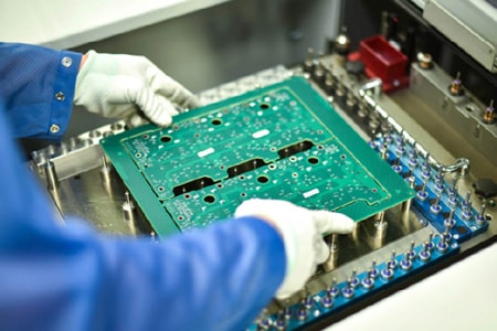
High-Precision Manufacturing Process

PCB Assembly
SMT & THT Assembly for Prototype to Volume
one-stop PCB BOM & Assembly Service
Free DFMReview Before Production
Prototype to Mass Production Support

Component Sourcing
Authorized & Traceable Electronic Components
700k parts with 100+suppliers
Customized solutions for components sourcing
Genuine ComponentsFully Traceable

Box Build Assembly
Complete Product Assembly & Integration
Cable & Harness Assembly
Enclosure Integration
Functional Testing Finished Product Delivery

From prototype to volume production, PCBAMake delivers fast, stable and quality-controlled assembly.
A clear PCBA workflow from file review and quotation to production, inspection and global delivery.
Flexible production planning for prototype, small batch and volume PCBA orders.
| Order Quantity | Standard | Quick Turn |
|---|---|---|
| Prototype & NPI Support (<100 pcs) | 5 Days | 1 Day |
| Small Volume Production (100–500 pcs) | 8 Days | 3 Days |
| Mid Volume Production (500–5000 pcs) | 10 Days | 5 Days |
| Large Production (>5000 pcs) | 15 Days | 7 Days |
Complete production files help our engineering and purchasing teams evaluate your PCBA project faster and more accurately.
| Capability | Standard |
|---|---|
| Certifications | ISO 9001: 2015, ISO14001: 2015, ISO13485: 2016, IPC, UL, Reach, RoHS |
| Lead Time | 1-5 days, as per the scheduled period |
| Parts Procurement | Full turnkey, partial turnkey, and kitted |
| Assembly Types | Surface Mount SMT, Through-hole, Mixed Technology, Single and double-sided SMT/PTH |
| Stencils | Laser cut stainless steel and Nano-coating |
| Components | Passive components smallest size 01005, Fine pitch components smallest size 8 mils pitch |
| Component Packaging | Reels, cut tape, tube, and loose parts |
| Inspection | X-ray analysis, AOI, and Microscope to 20X |
| Solder Type | Leaded and Lead-free / RoHS compliant |
| Assembly Surface Mount Connectors | Yes |
| Wave Soldering | Yes |
| PCB Finish | HASL, electrolytic gold, electroless gold, electroless silver, immersion gold, immersion tin, and OSP |
| Panelized PCB | Tab routed, breakaway tabs, v-scored and routed + v-scored |
| Rework | BGA removal and replacement station, SMT IR rework station, and through-hole rework station |
| Design File Format | Gerber RS-274D, Eagle, AutoCAD DXF, DWG, BOM, and pick and place file |

Certified processes for PCB manufacturing, assembly, inspection and global delivery.
From prototypes to volume production, PCBAMake supports demanding PCBA projects across medical, industrial, energy, communication and consumer electronics applications.

Support for high-reliability medical electronics with strict process control, traceable components, SMT assembly, inspection and functional testing requirements.

PCBA support for automation control, power modules and long-life industrial electronics requiring stable production quality.

Assembly solutions for chargers, power supplies and energy-related products with reliable soldering and inspection processes.

Support for communication modules, wireless devices and IoT hardware with fine-pitch SMT and mixed assembly capability.

From prototype samples to repeat production, supporting compact electronic products with fast response and flexible assembly.
End-to-end PCBA manufacturing with controlled processes and full traceability.


Send your Gerber files, BOM list, quantity and testing requirements. Our engineering and purchasing teams will review your project and provide a practical PCBA production plan.
Complete files help us evaluate cost, lead time, components and testing requirements more accurately.
Delivery Services

Verified by

Link Us on