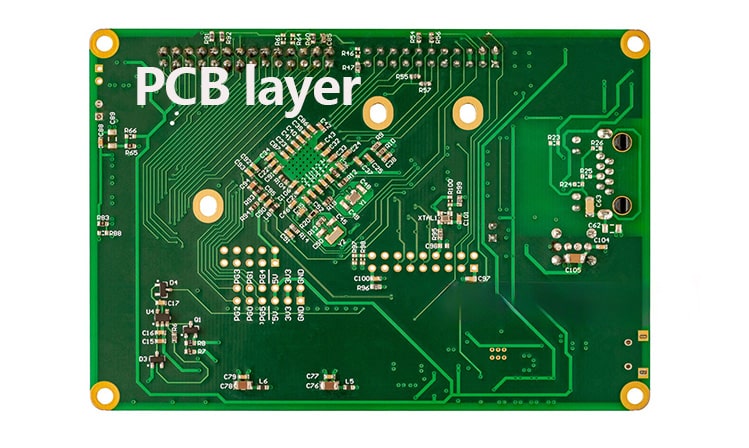
How to determine the number of PCB board layers
How PCB design determines the number of PCB layers. The efficiency of a PCB circuit board depends on the number of layers, so it is crucial to correctly select the number of PCB layers. So how do you decide the number of layers when designing PCB?

What does the number of PCB layers mean
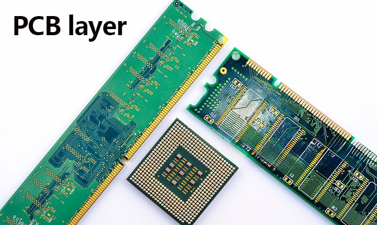
The layer of PCB refers to the copper layer. PCB is made of copper layer + base material. Except for single-sided boards, which are one layer of copper, boards with more than two sides are even-numbered layers. The components are welded on the outermost layer, and the other layers serve as wire connections. However, some high-end PCBs now bury components in the inner layer of the PCB.
PCBs are used in manufacturing various electronic devices and machinery in different industries such as consumer, automotive, telecommunications, aerospace, military, and medical industries. The number of layers and dimensions of a particular board determine the power and capacity of the PCB. As the number of layers increases, so does the functionality.
How to determine the number of PCB layers?
When you consider how to choose the number of PCB layers, you need to consider, what are the advantages of multi-layer compared to single-layer/double-layer? On the contrary, you also have to think about the advantages of single layer compared to double layer/multi-layer? Specifically, you can consider the following 7 aspects:
The following issues should be considered when deciding the number of PCB design layers:
1. Where is PCB used?
Before preparing to design a PCB, we need to understand where this PCB is used? And what are the requirements for PCB boards? It is necessary to consider the machines and equipment that the PCB will use, and also determine the requirements of these machines/equipment for the circuit board circuit. Is it for high-tech, complex electronics or simpler products with fewer features?
2. What operating frequency does PCB require?
The parameters of the operating frequency determine the functionality and capacity of the PCB. The choice of the number of layers also depends on the type of signal they need to carry. Signals are classified into high frequency, low frequency, ground or power. For applications that require multiple signal processing, a multi-layer PCB is required. These circuits may require different grounding and isolation.
3.Through hole type
Via selection is another important factor to consider. If you choose to bury vias, more internal layers may be required, so multi-layer needs can be accommodated accordingly.
4. Density and number of signal layers required
The determination of PCB layers is also based on two important factors: signal layer and pin density. The number of layers in a PCB increases as pin density decreases. Pin density is 1.0. For example, a pin density of 1 would require 2 signal layers. However, pin density <0.2 may require 10 layers or more.
5. Number of planes required
Power and ground planes in PCBs help reduce EMI as well as shield signal layers. Therefore, the choice of layers will again depend on the number of planes required.
6. Manufacturing cost
Although a primary requirement, it is one of the determining factors in choosing the number of layers in a 1-40 layer PCB design. The cost of PCB manufacturing depends on the multiple layers. Multi-layer PCBs are more expensive than single-layer PCBs and the manufacturing cost will largely depend on the above requirements.
7. Delivery time
Delivery time is the time required to manufacture single-layer/double-layer/multi-layer PCB boards. When you need to manufacture PCB boards in large quantities, you need to take the delivery time into consideration. The delivery time of single-layer/double-layer/multi-layer PCB boards is also different, depending on the size of the PCB board area. Of course, if you are willing to spend more money, the delivery time may also be shortened.

Delivery time based on 1-40 layer PCB manufacturing designs depends on all the above factors. Usually PCB designers will judge the design of several layers of boards based on the complexity of the designed circuit schematic diagram, mainly based on the routing of core components in the schematic diagram and the difficulty of device layout. If you are unable to make a decision based on the above factors, it is best to discuss it with the manufacturer.

