- Home
- About us
- Products
- PCB Fabrication
- PCB Assembly&OEM
- Quality
- Blogs
- Contact
One-Stop Turnkey PCB Assembly Manufacturer
PCB Assembly&OEM

BGA PCB Design DFM: Manufacturing Risks and Optimization Strategies
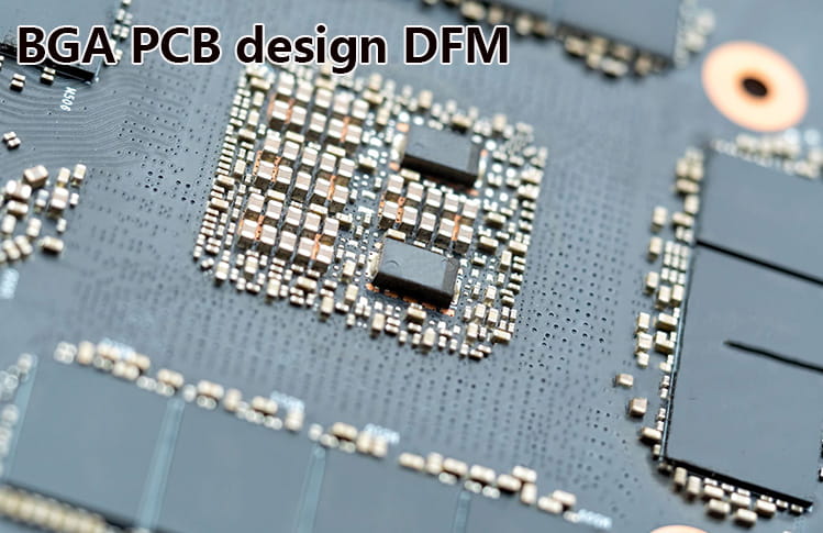
BGA packages enable high I/O density but also introduce significant manufacturing risks.
In many cases, BGA soldering issues originate from PCB DFM weaknesses, not assembly errors.
Common Manufacturing Risks in BGA PCB Design
Insufficient solder mask clearance
Improper via-in-pad implementation
Inconsistent thermal balance
Without proper DFM, these issues often surface during mass production.

Critical DFM Considerations for BGA PCBs
1. Via-in-Pad Design Decisions
Via-in-pad can improve routing density but requires:
Proper copper filling
Planarization control
Incorrect implementation leads to solder voiding and reliability problems.
2. Solder Mask Design for High-Density BGAs
Extremely narrow solder mask bridges increase:
Risk of solder bridging
Mask misalignment defects
DFM recommends maintaining manufacturable solder mask openings, even if it slightly increases layout area.
3. Thermal Balance and Warpage Control
Uneven copper distribution under BGAs may cause:
Warpage during reflow
Head-in-pillow defects
Balanced copper design improves both assembly yield and long-term reliability.
4. Inspection and Rework Accessibility
High-end BGA designs should consider:
AOI and X-ray inspectability
Rework feasibility
Designing for inspection is a critical but often overlooked DFM factor.
👉 Related reading: High Precision PCB DFM Checklist
BGA DFM as a Reliability Strategy
For products requiring long lifecycle stability, BGA DFM directly impacts field reliability.
Well-planned DFM reduces rework dependency and improves overall manufacturing confidence.If you have PCB/PCBA/OEM/ODM needs, please contact us, We will reply within 2 hours, and complete the quotation within 4 hours or less upon request.