
 Orders@pcbamake.com

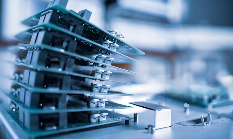
What is PCBA post-welding processing?
PCBA post-welding processing refers to the manual soldering of electronic components that are not suitable for wave soldering after the circuit board has undergone wave soldering. The purpose of post-welding processing is to compensate for the shortcomings of wave soldering and improve soldering efficiency.
In PCBA processing, wave soldering is a common soldering method, but some components cannot be completed by wave soldering due to their high temperature resistance, high temperature, or proximity to process edges. In this case, post-welding processing is required to perform repair welding to ensure the normal operation of the PCB manufacturing.
The advantage of post-welding processing is that it can be used to repair components that are not suitable for wave soldering, while ensuring the quality and efficiency of the welding process. During post-welding processing, manual soldering using an electric soldering iron is required, which places high demands on the skills and experience of the operator. Therefore, when processing PCBAs, it is necessary to select the appropriate soldering method and operator based on the different components and soldering requirements to ensure the quality and efficiency of the welding process.
In short, PCBA post-welding processing is a very important soldering method in PCBA processing, which can compensate for the shortcomings of wave soldering and improve soldering efficiency. When selecting the appropriate soldering method and operator, it is necessary to consider different components and soldering requirements to ensure the quality and efficiency of PCBA soldering.
If you have PCB/PCBA/OEM/ODM needs, please contact us, We will reply within 2 hours, and complete the quotation within 4 hours or less upon request.
Delivery Services

Verified by

Link Us on


