Orders@pcbamake.com


Most of the PCBs we usually see are rigid PCBs
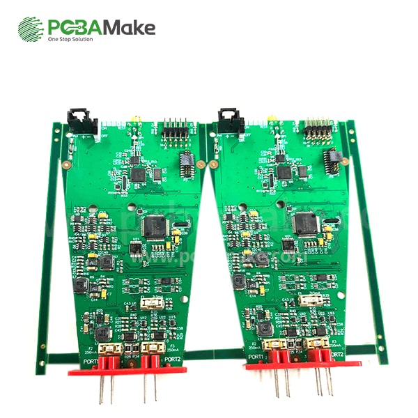
5G PCBA
Material: FR4
Finish treatment: Immersion Gold
Copper thickness: 1oz~ 2oz
Resin plugging vias & Buried vias
Impedance Controller Board
5G technology has been a topic that everyone pays close attention to since its inception. Since 2020, 5G has become very popular, and the era of the Internet of Everything is coming.
The development of 5G has promoted the construction of large-scale data centers, which means that a large number of high-end PCB communication boards will be required to support the huge traffic carried by the data center servers. Therefore, the requirements for the number of layers and materials of multi-layer PCBs will also increase. high. Undoubtedly, the development of 5G drives the multilayer PCB board to the direction of high precision and complexity.
What challenges does 5G communication bring to the PCB industry
Requirements for materials: A very clear direction for 5G PCB is high-frequency and high-speed materials and boards. This will break the current situation of Rogers' dominance in the field of high-frequency sheets, and will greatly enhance the requirements for the performance, convenience and availability of materials.
Requirements for quality monitoring: With the increase of 5G PCB signal rate, the impact of board manufacturing deviation on signal performance has become greater, and the production deviation control of board manufacturing has become more stringent.
Requirements for process technology: The functional improvement of 5G PCB-related application products will increase the demand for high-density PCBs, and HDI PCB will also become an important technical field. Multi-stage HDI PCB products and even products interconnected in any order will be promoted, and new processes such as buried resistance and buried capacity will be used more and more.
Requirements for 5G PCB design: The selection of the board must meet the requirements of high frequency and high speed, and the impedance matching, stacking planning, wiring spacing/holes, etc. must meet the signal integrity requirements.
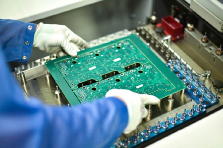
Requirements for equipment and instruments: high-precision equipment and pre-processing lines with less roughening of the copper surface are the ideal processing equipment at present; and the test equipment includes passive intermodulation tester, flying probe impedance tester, loss test equipment, etc. .
Precise pattern transfer and vacuum etching equipment, detection equipment for line width and coupling spacing that can monitor and feedback data changes in real time; electroplating equipment with good uniformity, high-precision lamination equipment, etc. can also meet the production needs of 5G PCB.
1- 40 layer PCB/PCBA/EMS/OEM/ODM | One stop solution
We can provide PCB assembly services in custom specifications to meet your application requirements.
Delivery Services

Verified by

Link Us on