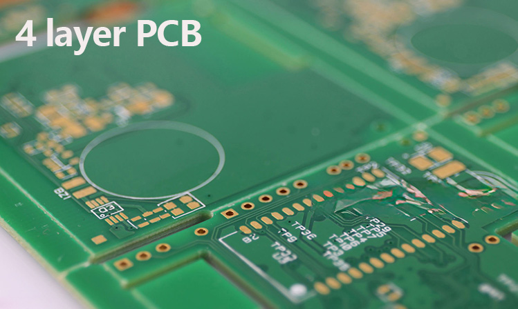
Everyone is familiar with PCB. The most common and widely used one is the 4 layer PCB.
Multilayer PCB is the result of the development of electronic information technology towards high speed, multi-function, large capacity, small volume, thinness and lightweight. For the production of PCB boards, the more layers there are, the more procedures are required, the failure rate will increase accordingly, and the corresponding cost will be higher. Therefore, multilayer boards are generally used in advanced circuits. 4 layer PCB is a common multi-layer PCB, so what are the four layers of a 4 layer PCB?
4 layer board structure
The 4 layer PCB board is composed of four different layers, signal layer (top layer), signal layer (bottom layer), power layer (middle layer) and ground layer (middle layer). Each layer has different functions and roles. These layers are connected through holes and vias on the circuit board to achieve communication and transmission between various parts on the circuit board.

The functions and roles of each layer
1. Top layer: The top layer is the top layer of the 4 layer PCB board. It contains most of the components and circuits, including power supplies, signal lines, ground wires, crystal oscillators, etc. The top layer is also the layer that has the closest contact with users, so special attention needs to be paid to its arrangement and wiring when designing.
2. Bottom layer: The bottom layer is the lowest layer of the 4 layer PCB board. It is usually used to place some larger components and connectors. The bottom layer also contains components and circuits such as power supply, signal lines, and ground wires.
3. Internal layer 1: Internal layer 1 is the internal layer closest to the top layer of the 4 layer PCB board. It is mainly used to connect signal lines and power lines between the top layer and the bottom layer. The layout and routing of internal Layer 1 has a significant impact on circuit performance and electromagnetic compatibility.
4. Internal layer 2: Internal layer 2 is the internal layer closest to the bottom layer of the 4 layer PCB board. It is mainly used to connect signal lines and power lines between the bottom layer and the top layer. The layout and routing of internal Layer 2 also has a significant impact on circuit performance and electromagnetic compatibility.
How to design an efficient 4 layer board
We need to consider the following aspects when designing an efficient 4 layer board:
1. Level planning and layout;
2. Wiring of signal lines and power lines;
3. The location and number of through holes and vias;
4. Arrangement and packaging of components.
4 layer PCBs play an important role in modern electronic design, and their multi-layer structure provides higher signal integrity and power stability. Through reasonable structural design and strict manufacturing control, 4 layer PCB boards can meet the needs of complex circuits and play a key role in high-performance electronic devices. If you have 4 layer board needs, please feel free to contact us.
If you have PCB/PCBA/OEM/ODM needs, please contact us, We will reply within 2 hours, and complete the quotation within 4 hours or less upon request.